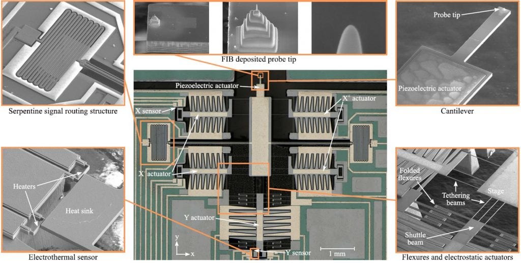
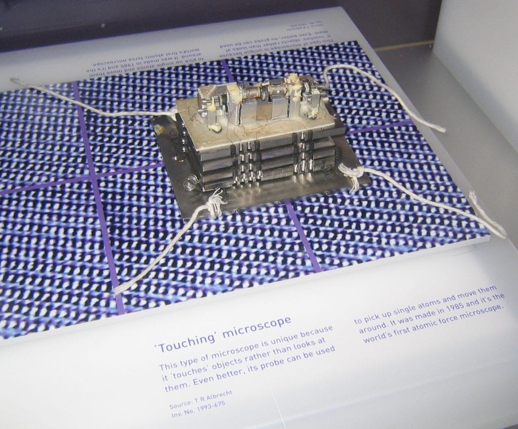
An atomic force microscope is one of the instruments that made nanotechnology feasible and now costs half a million dollars, now it fits into a chip.
What is an atomic force microscope?
An atomic force microscope (AFM) is a scientific tool used to generate detailed three-dimensional images of the surfaces of the materials, up to the nanometer scale – which is approximately in the scale of the individual molecules. This equipment, developed by Gerd Binnig and Heinrich Rohrer in the early 1980s, has demonstrated resolution in the order of fractions of a nanometer.
What is this device for?
The AFM is an instrument that “allows” the existence or that facilitates the advancement of nanotechnology today. Currently, an atomic force microscope costs half a million dollars. Originally it had a dimension similar to a smartphone, but now it fits inside a chip. This miniaturization was possible with the use of a MEMS (Microelectromechanical System), a microelectromechanical system. An MEMS-based atomic force microscope developed by engineers at the University of Texas at Dallas is about 1 centimeter square in size. University officials say an educational version of the device costs $30,000 to $40,000. When you move to a lab level, the price goes up to $500,000. Dr. Reza Moheimani, professor of mechanical engineering at UT Dallas said that “A conventional atomic force microscope is a large, bulky instrument with multiple control meshes, electronics, and amplifiers.” One of the objectives of this research is to produce mass production to reduce the complexity and cost of the instrument significantly. One of the attractive aspects about MEMS is that it can be mass-produced, making hundreds or thousands of them at once. That way the price of each chip would be only a few dollars. As a result, it will be possible to offer the entire miniature atomic force microscope system for a few thousand dollars. But the “trivialization” of production will also make the microscope have a “consumer” price. An AFM is a microscope that ‘sees’ a surface similarly as a visually impaired person ‘sees,’ that is, by touch. A tiny arm, fixed on one side and with a sharp tip at the end, is moved back and forth along the surface of the sample – or else the sample moves over the small silicon or diamond tip. The forces of interaction between the tip of the microscope and the specimen cause the tip to move up and down. These movements are then converted into a topographic image.
AFM on a chip
The AFM on a chip measures about 1-centimeter square, with the MEMS attached to a circuit board which is about a size of a credit card. This board contains all the circuits, sensors and other components necessary to control the movement of the device. The prototype still does not rival the quality of the images of the commercial devices, but the team claims that it is a first generation production, in which they continue to work until a possible result of commercialization comes. So, what do you think about this AFM? Share your views and thoughts in the comment section below.

